|
Main
products:
CNT AFM Probes Series
(cnt probe selection)
Advantages
of CNT AFM probe (碳纳米管探针优点):
1.Very long
lifetime, very high resolution (超长使用寿命,超高分辨率)
2.High
repeatability (一致性好,无需频繁换针)
3.Lower cost
(使用成本更低)
►
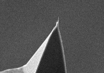
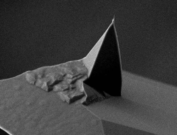
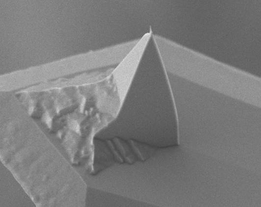
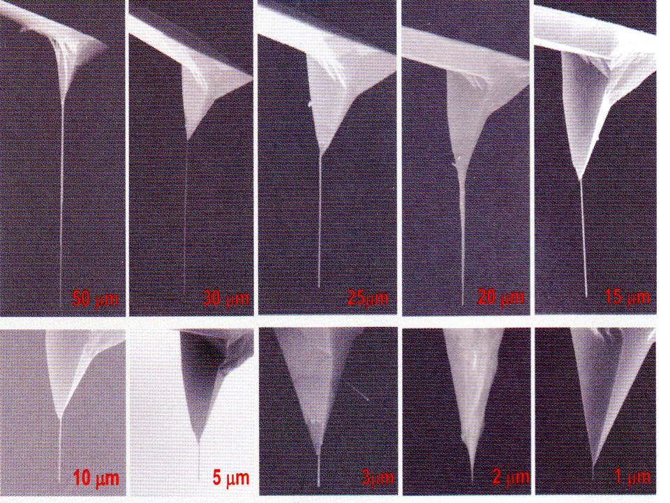
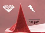
碳纳米管原子力显微镜探针
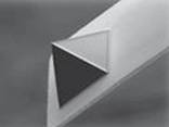
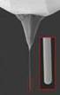
扫描成像效果展示图
Imaging by our CNT probe
High resolution and
Trench imaging by CNT AFM probes
CNT
probes from us include two series: high resolution and
high aspect ratio applications.
Tip
features:
-
A
carbon nanotube/nanocone of 2 nm radius of
curvature right at the apex of regular silicon
probe,either tapping or contact mode.
-
Probe
with perfect alignment,orientation of CNT is better
than ±5º.
-
Tightly
controlled CNT length, 0.6µm±200nm, 1.5µm±200nm,
5µm±500nm
-
Extremely
high resolution and long lifetime.
纳米线
原子力显微镜探针 AFM probe
导电纳米线探针:导电性能好,一致性高,长寿命!
制备工艺:
通过在原子力显微镜探针(国际通用的普通硅探针)上可控生长纳米线得到。
纳米线材料:
导电金属材料
纳米线探针尺寸:
20-50纳米半径,长度为1-3微米,5-8微米等多种规格,也可以为客户定制。
应用:
EFM,voltage Lithography,Surface potential imaging,
Rheological measurement,SECM,F-D microscopy on soft
materials
(cell probing, liquid property measurements)
公司产品包括以下世界著名品牌:
    
NANOSENSORS
was the first company to commercially manufacture AFM
probes. Now NANOSENSORS provide high quality AFM probes for
reproducible measurement results.
AppNano
providing high quality probe for various applications.
非接触/轻敲模式针尖(Non-contact
/ Dynamic mode/Tapping mode AFM probes)原子力显微镜探针
技术参数:
针尖材料: 高掺杂单晶硅
外观尺寸:
3.4x1.6x0.3 mm
针尖形貌:
金字塔型
针尖高度: 15
μm
反光镀层 (可选):
铝或金
针尖半径:~10nm (tip
radius)
Force Constant: ~45 N/m;Resonant
Frequency: 180-350 kHz
特点:常用的产品,分辨率高,使用寿命一般
接触模式针尖(Contact
mode AFM probes)原子力显微镜探针
技术参数:
针尖材料: 高掺杂单晶硅
外观尺寸:
3.4x1.6x0.3 mm
针尖形貌:
金字塔型
针尖高度: 15
μm
反光镀层 (可选):
铝或金
针尖半径:~10nm (tip
radius)
Force Constant: 0.05-3N/m;Resonant
Frequency:10-40 kHz
特点:常用的产品,分辨率高,使用寿命一般
导电原子力显微镜探针,磁性原子力显微镜探针
导电针尖通过对普通针尖镀10-50纳米厚金属
层得到。
轻敲模式,力调制模式都可使用导电针尖。
特点:常用产品,分辨率一般,使用时导电镀层容易脱落,从而影响导电性/磁性和寿命
导电针尖的新产品有碳纳米管针尖,金刚石镀层针尖,全金刚石针尖,全金属丝针尖,这些新技术克服了普通导电针尖的短寿命和分辨率不高的缺点。
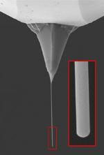
大长径比原子力显微镜探针是专为测量深的沟槽以及近似铅垂的侧面而设计生产的。
 
技术参数:针尖高度:
> 9 μm;长径比: 5:1;针尖半径:
< 10 nm
特点:不太常用的产品,分辨率很高,使用寿命
很短
其他特殊探针和针尖
化学力显微镜针尖(Chemical
Force Microscopy)
磁力显微镜针尖 (Magnetic
Force Microscopy)
压痕仪针尖(Nano Indentation)
无针尖悬臂 (Tipless
Cantilevers)
Other
SPM related products
隔震平台
Nano-K Vibration Isolation Platforms
Nano-K bench top systems offer the highest level of
vibration isolation performance possible for Scanning Probe
Microscopes (AFM and STM). Featuring a totally passive
1/2-Hz system, they outperform air systems by 10 to 100
times. The use of superior, leading-edge, negative-stiffness
technology results in a cost-effective, compact, lightweight
system that is easy to adjust and has no facility
requirements. These features make them perfect enabling
accessories for high performance vibration sensitive
instruments.
SPM
software
The Scanning Probe Image Processor
SPIP is the industry-leading image analysis software for
Scanning Probe Microscopy (SPM) and supports virtually every
SPM file format. It is also the preferred analysis software
for other types of nano and micro-scale imaging - such as
SEM and TEM, confocal and optical microscopy, interferometry
and profilometry. SPIP's modularity allows you to choose
only the modules that you need for your current research,
thus minimizing your cost while providing an option for
future upgrades.
Standards
and calibration samles
|